
Atomic resolution for everybody?
[Chromatic correction: A revolution in electron microscopy Speech held by Joachim Zach at the Royal Society of Microscopy 2009 in London]
Basics
The invention of the electron microscope promised a large advance in resolution compared to optical microscopy, because the electron wavelength at reasonable acceleration voltages is very much smaller than the wavelength of light.
\lambda=\frac{h}{\sqrt{2{m_\omicron}eU}}
According to de Broglie one can assign the wavelength λ to an electron which is accelerated by U [h Planck's constant, e elemental charge, m0 rest mass of the electron].
For example an electron accelerated by 10 kV behaves like a wave of wavelength 0.012 nm, its velocity equals 10% of the velocity of light. A further increase in acceleration voltage requires the application of the relativistic corrected formula.
\lambda=\frac{h}{\sqrt{2{m_\omicron}eU}}\cdot\frac{1}{\sqrt{1+\frac{eU}{2{m_\omicron}c^2}}}
Being accelerated by 200 kV the electron reaches 70% of the speed of light, its resulting wavelength is 0.0025 nm.
d=N\cdot\frac{\lambda}{sin\space\alpha}
The theoretical resolution limit d can be calculated at given wavelength λ and half angle of beam spread α (which is determined by the beam aperture). N is a factor of about one, its exact value depends on the applied resolution criterion.
Uncorrected microscopes usually operate at half angle of beam spread of about 10 mrad, this reduces the theoretical resolution limit to 100 times the electron wavelength (0.25 nm). Microscopes with a built-in corrector achieve an half angle of beamspread up to 50 mrad resulting in a resolution limit of 0.05 nm.
Unfortunately the electron-optical lenses exhibit rather poor optical properties (aberrations), which prevent to achieve the theoretical resolution limit. The major amounts to the aberrations are contributed by chromatic and spherical aberration. Coefficients Cs and Cc given the resolution limit can be calculated from the following equations (A and B are multipliers of scale one according to N):
spherical aberration
d_s=B\cdot\sqrt[4]{\lambda^3\cdot{C_3}}
chromatic aberration
d_c=A\cdot\sqrt{\lambda\cdot\frac{\Delta{E}}{E}\cdot{C_c}}
These formulas make clear that resolution is determined by the following microscope properties:
- the acceleration voltage U defines λ and via the relation E=e·U also the energy width ΔE/E.
- the focal length of the objective lens determines the aberration coefficients
- the source is the crucial factor for the energy width of the electron beam ΔE/E
Proceeding in a conservative way
From a historical point of view the development of electron microscopy during the last 30 years was pushed by the desire to optimize the resolution in spite of lens aberrations. The parameters used were those cited above, which we will explain in the following:
Applying a very high acceleration voltage
In order to obtain very high acceleration voltages (bigger than 1 MV) one has to build giant machines necessitating a building of their own. There exist only a handful of these instruments all over the world.
Using strong objective lenses with short focal lengths:
The only free parameter to reduce the spherical aberration is the spherical aberration coefficient, the magnitude of which is given by the focal length of the objective lens. In case of immersion (e.g. the specimen is situated within the lens field) it is reduced to half of the focal length. But due to the spatial conditions the focal length cannot be reduced to less than 1 mm. Besides several drawbacks of strong focal lenses have to be pointed out:
- they reduce the space in which the specimen can be handled
- they require expensive and sensitive material in order to minimize saturation effects
- they are implemented by thick coils which need a lot of space and whose dissipation necessitates a complex cooling mechanism
Reducing the energy width:
Novel electron guns exhibiting small energy widths as for example Schottky- or field emission guns require a complex vacuum technology (ultra high vacuum). Using these sources without chromatic error could yield atomic resolution already at 200 kV.
The silver bullet of correction
Otto Scherzer suggested already in the 1940s to compensate the lens aberrations by using non-rotational symmetric elements. The first goal of the scientists was to counterbalance spherical aberration. In the 1960s electric/magnetic quadrupoles were used. After the Darmstadt project (more information here) had been in progress for about ten years, it was shown for the first time that spherical AND chromatic aberration could be compensated in principle by using a quadrupole/octupole corrector. It was not before 1995 when it could be shown by Haider and Zach using a low-voltage SEM that aberration correction improves resolution.
In October 2008 the next milestone was reached. CEOS implemented a spherical and chromatic aberration corrector in a TEM, which has been disposed for Argonne National Laboratory within the scope of the TEAM project.
Given that spherical and chromatic aberration correction is available now for both TEM and SEM it is possible to dispense with all those self-imposed constraints and get nevertheless atomic resolution by aberration-free imaging.
Definition of aberration free imaging (AFI)
When the main aberrations are corrected the remaining aberrations of higher order lead to a certain phase shift of the electron wave. In our definition of aberration free imaging the resulting phase shift of all aberrations of a certain annular multiplicity should not exceed Π/4. This must be valid for the whole range of spatial frequencies which is necessary for the resolution aimed for.
A revolution on the horizon
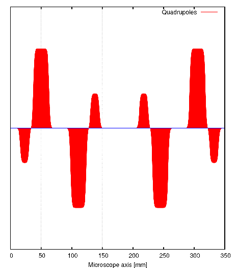
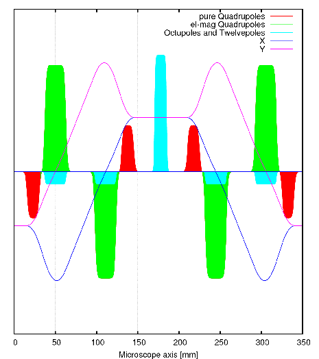
The order of optical elements within the corrector is depicted schematically. The setup is mirror symmetric with respect to a central plane to reduce off-axial aberrations.
The units are chosen arbitrarily.
The path of rays is formed by quadrupoles. The excitations can be kept quite low, even at an acceleration voltage of 200 kV the magnetic excitation may rest well below 25 ampturns.
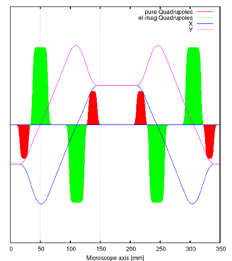
The beam path shows four astigmatic intermediate images in the correction pieces (see also correction principle below).

The octupoles and dodecapoles in the correction pieces and in the central multipole are depicted in turquoise colour.
Principle of correction
- correction of chromatic aberration: electro-magnetic quadrupoles in the correction pieces (principle of a first order Wien filter - as realised in 1995 by Zach/Haider for the first successful corrector).
- correction of spherical aberration: octupoles and dodecapoles in the correction pieces
- correction of four- and six-fold astigmatism: octupole and dodecapole in the central multipole
The remaining aberrations lead to phase shifts, the sum of which fulfills the criterion for aberration free imaging for 0.05 nm resolution.
Atomic resolution can be realised in a corrected 200 kV electron microscope.
Low voltage microscope with atomic resolution
In order to achieve atomic resolution one can dispense with high beam energies if the microscope is corrected. The question we want to discuss now is how much the acceleration voltage can be decreased delivering nevertheless a resolution of 0.1 nm.
We scale down the whole system to 30 kV and discuss its properties. Assuming a LaB6-gun we calculate the remaining phase shifts. Except of the star aberration of 7th order they all meet the AFI criterion. Even this phase shift can be halved by compensating it with the well-known 2-fold astigmatism.
Atomic resolution of 0.1 nm can be realised with a corrected 30 kV electron microscope.
Standard-TEM with atomic resolution
For a long time the standard TEM has been an instrument operating at 100 kV, making use of a simple gun, for example a LaB6-gun. Assuming an energy width of 1 eV we have calculated the resulting phase shifts. According to our calculations atomic resolution can be achieved without any difficulties.
The performance of uncorrected high-end instruments can also be achieved by using a simple and cheap microscope.
Simple far field objective lens with atomic resolution
In the past excellent resolution could only be expected in transmission microscopes with very strong objective lenses. But that meant squeezing the specimen into the tiny gap between the pole pieces and exposing it to a vast magnetic field.
In contrast to that a corrected microscope offers the possibility to use a weak objective lens, where the specimen is placed outside the magnetic field. We have modelled a corrector, where the whole arrangement of lens and corrector requires only 35 cm. This is less space than needed by a strong objective lens without corrector.
In this case a resolution of 0.1 nm is difficult to achieve in practice because it would require detailed counterbalancing of various aberrations of 7th order by aberrations of lower order. However, already a target resolution of 0.11 nm can be achieved meeting the AFI-criteria, the counterbalancing can be done almost unperceived by defocussing.
It has to be admitted that such an arrangement offers the disadvantage of very high stability requirements. But it should be noted that those requirements are of the same order as the ones which are fulfilled for the TEAM project. For high magnifications it may be necessary to incorporate an additional lens because of the large focal length.
Perspective
Since chromatic and spherical aberration correction is both feasible for electron microscopes now, the manufacturers have won further degrees of freedom. Many restrictions which have been indispensable for a good resolution up to now can be dispensed with. The "cheaper" instruments offered by microscope manufacturers today have already a lattice resolution up to 0.14 nm. In many cases resolution is limited by chromatic aberration, so that incorporating a suitable corrector would lead to atomic resolution. A relative stability of 10-7 at least would be sufficient. Therefore "atomic resolution for everybody" could become reality soon.